全球超过 60,000 名订阅用户
支持与服务
标准版
《Cursor - 人工智能代码编辑器》
企业版
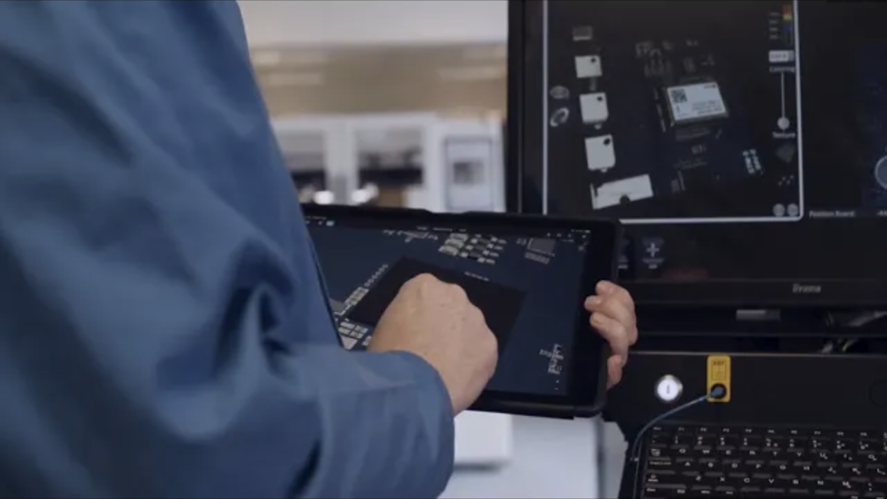
奥腾设计软件
Standard
Pro
Enterprise
软件更新  Maintain access to the latest Altium Designer updates as they are released.
Maintain access to the latest Altium Designer updates as they are released. 
统一设计环境
Provides a single environment for every aspect of the PCB design process including schematic capture, PCB layout, multi-board assembly, harness design, library management, simulation, documentation, and more.
多站点许可证支持
Standard
Pro
Enterprise
单站点 This license type can be used in one location only. Learn More
This license type can be used in one location only. Learn More 大陆 This license type can be used within one continent. Learn More
This license type can be used within one continent. Learn More 
全球 This license type can be used anywhere. Learn More
This license type can be used anywhere. Learn More 原理图捕获
Standard
Pro
Enterprise
层次化与多通道设计
Enables the creation of designs at a block diagram top-level, where projects can be split into manageable logical chunks. Hierarchical design also allows you to create multiple copies of the same block when you need multiple channels of an identical circuit. 原理图设计规则 Use automated rules that help you to correctly lay out a PCB. Design rules can be added to schematics for nets, wires, busses, harnesses, components, sheets, or document parameters.
Use automated rules that help you to correctly lay out a PCB. Design rules can be added to schematics for nets, wires, busses, harnesses, components, sheets, or document parameters. 电气规则检查 Helps prevent design mistakes by alerting you to problems in a schematic like electrical faults. These validation checks will be performed after any change is made to a design and on every release.
Helps prevent design mistakes by alerting you to problems in a schematic like electrical faults. These validation checks will be performed after any change is made to a design and on every release. 设计流程自动化
Add cross-references to a project that allow you to easily follow the connective flow of nets between the schematic sheets in a project. All sheets are automatically numbered to help keep your designs organized. 设计导入器 Leverage previous designs to reduce time re-creating schematics, board layouts, and associated design data with an automatic importer of project files from your preferred PCB design tool. Supports P-CAD®, Autodesk® EAGLE™, Cadence® Allegro®, Cadence® OrCAD®, KiCad®, LTspice®, Mentor Graphics® DxDesigner®, Mentor Graphics® Expedition®, Mentor Graphics® PADS®, Mentor Graphics® xDxDesigner®, Simbeor®, Zuken® CADSTAR®, and Zuken® CR-5000®.
Leverage previous designs to reduce time re-creating schematics, board layouts, and associated design data with an automatic importer of project files from your preferred PCB design tool. Supports P-CAD®, Autodesk® EAGLE™, Cadence® Allegro®, Cadence® OrCAD®, KiCad®, LTspice®, Mentor Graphics® DxDesigner®, Mentor Graphics® Expedition®, Mentor Graphics® PADS®, Mentor Graphics® xDxDesigner®, Simbeor®, Zuken® CADSTAR®, and Zuken® CR-5000®. 仿真
Standard
Pro
Enterprise
Ansys 协同设计 Digital connection between Altium software and Ansys Electronics Desktop (AEDT) to enable streamlined exchange of data and seamless collaboration between electrical and simulation engineers, replacing manual and error-prone data exchange and communication methods.
Digital connection between Altium software and Ansys Electronics Desktop (AEDT) to enable streamlined exchange of data and seamless collaboration between electrical and simulation engineers, replacing manual and error-prone data exchange and communication methods. 集成 SPICE 仿真
Create and manage multiple simulation profiles. Separate profiles allow you to run different types of analyses with different simulation engines (e.g., Mixed Sim, SIMetrix, SIMPLIS). This enables multiple runs of the same simulation type (e.g., AC or DC analysis) with different parameters and options (e.g., different frequency ranges). LTSpice 导入器 Simulation designs saved from LTspice® can be imported into Altium Designer with the LTSpice Import Wizard. Component symbol files referenced by the LTSpice design file (*.asc) are automatically added as library files, and in turn, the simulation models referenced within the component library files are also added to the import.
Simulation designs saved from LTspice® can be imported into Altium Designer with the LTSpice Import Wizard. Component symbol files referenced by the LTSpice design file (*.asc) are automatically added as library files, and in turn, the simulation models referenced within the component library files are also added to the import. 电路板布局
Standard
Pro
Enterprise
PCB 协同设计 Allows engineers and teams to work simultaneously on the same project, enabling engineers to dramatically compress design cycles and accelerate the overall design process.
Allows engineers and teams to work simultaneously on the same project, enabling engineers to dramatically compress design cycles and accelerate the overall design process. 规则驱动设计 Define specific manufacturing guidelines with a customizable design rule system including specifications for board outlines, solder mask expansions, drill placement, and an advanced query editor to create non-standard rules.
Define specific manufacturing guidelines with a customizable design rule system including specifications for board outlines, solder mask expansions, drill placement, and an advanced query editor to create non-standard rules. 可视化层堆栈管理
Define the material composition and specialized regions on a board. For flex circuitry, rigid-flex, and embedded technology PCB designs, you can control the entire stackup, including all rigid and flex portions with bending angles and individual layer definitions. You can visualize layer stacks using subsets of materials used in the primary layer stack, and each layer has an individual definition and corresponding parametric data from a Materials Library. 约束管理器 Centralizes rules and constraints management with a unified table-based editor in both the schematic and PCB editors consolidating all electrical and physical design rules. Constraint sets can be reused between designs to save time when constraining new projects.
Centralizes rules and constraints management with a unified table-based editor in both the schematic and PCB editors consolidating all electrical and physical design rules. Constraint sets can be reused between designs to save time when constraining new projects. 材料库 Define system-wide parametric data on any materials you may specify in the construction of your layer stack. You can create any new material you intend to use, or use the set of generic ones already available, and the materials library can be saved and loaded to XML - so you can share it with your entire team.
Define system-wide parametric data on any materials you may specify in the construction of your layer stack. You can create any new material you intend to use, or use the set of generic ones already available, and the materials library can be saved and loaded to XML - so you can share it with your entire team. 高密度互连设计 Enables accurate design and visualization of HDI structures, including laser-drilled and mechanical microvias, stacked microvias, and skip-vias. A dedicated Layer Stack Manager allows you to define what µVia, blind/buried and other via structures you can allow in your project, and control the layer stack symmetry accordingly.
Enables accurate design and visualization of HDI structures, including laser-drilled and mechanical microvias, stacked microvias, and skip-vias. A dedicated Layer Stack Manager allows you to define what µVia, blind/buried and other via structures you can allow in your project, and control the layer stack symmetry accordingly. 3D-MID 设计 Currently in open beta. Create a non-planer design (3D-MID) by synchronizing components and connectivity from the schematic into a new dedicated layout type, and edit directly on the surface of a 3D substrate. You can export the manufacturing data in the format required by the Laser Direct Structuring process. Learn more
Currently in open beta. Create a non-planer design (3D-MID) by synchronizing components and connectivity from the schematic into a new dedicated layout type, and edit directly on the surface of a 3D substrate. You can export the manufacturing data in the format required by the Laser Direct Structuring process. Learn more 铜皮管理 Create areas of copper for power and signal planes that can be defined using three different design objects: Fills, Solid Regions and Polygon Pours. You can control the placement (pour) order and temporarily disable (shelve) regions to make it easier to see your underlying PCB layout.
Create areas of copper for power and signal planes that can be defined using three different design objects: Fills, Solid Regions and Polygon Pours. You can control the placement (pour) order and temporarily disable (shelve) regions to make it easier to see your underlying PCB layout. 精确对象放置
Facilitate routing and avoid physical collisions with the use of rooms, keepouts, and polygon regions to aid you when designing. Rooms are regions that assist in the placement of components by grouping them inside a designated area. Keepout regions act as an ‘interference’ object that prevents other copper objects from intersecting its area. 刚柔结合设计 Design today’s flexible circuitry in full 3D as part of a complete electronics product. Allows you to confirm that 3D components, case assembly, and PCB clearances meet your manufacturing requirements in real-time. Layer Stack Regions allow a single board to be composed of multiple materials, flexibility, and thickness, enabling the design of Rigid-Flex-Rigid PCB assemblies.
Design today’s flexible circuitry in full 3D as part of a complete electronics product. Allows you to confirm that 3D components, case assembly, and PCB clearances meet your manufacturing requirements in real-time. Layer Stack Regions allow a single board to be composed of multiple materials, flexibility, and thickness, enabling the design of Rigid-Flex-Rigid PCB assemblies. 高速设计 Design high-speed electronics with a powerful tuning engine. Includes advanced pattern support, an EM solver for accurate propagation delay, impedance extraction, and Easy HDI structure integration.
Design high-speed electronics with a powerful tuning engine. Includes advanced pattern support, an EM solver for accurate propagation delay, impedance extraction, and Easy HDI structure integration. 阻抗配置文件 Accurately control trace impedances (single and differential pairs) to maintain signal integrity in your high-speed designs. Impedance profiles use a fast, accurate 2D field solver to calculate impedances from trace widths, and trace widths and spacings from impedances. Single-ended and differential microstrip or striplines including asymmetric planes can be specified using plane layers or signal layers as references.
Accurately control trace impedances (single and differential pairs) to maintain signal integrity in your high-speed designs. Impedance profiles use a fast, accurate 2D field solver to calculate impedances from trace widths, and trace widths and spacings from impedances. Single-ended and differential microstrip or striplines including asymmetric planes can be specified using plane layers or signal layers as references. 反钻孔支持 Provide room for screw heads in a PCB laminate. You can add one counterbore or countersink hole per pad in a PCB design. This capability is supported in 2D, 3D, and in manufacturing drawings.
Provide room for screw heads in a PCB laminate. You can add one counterbore or countersink hole per pad in a PCB design. This capability is supported in 2D, 3D, and in manufacturing drawings. PCB 布局复制 Easily duplicate layouts for repetitive circuit blocks by transferring the design structure from one group of components to another identical group. Fragments of a PCB with the same components and connectivity are instantly identified and then copied without having to worry about managing reuse blocks or manually matching components.
Easily duplicate layouts for repetitive circuit blocks by transferring the design structure from one group of components to another identical group. Fragments of a PCB with the same components and connectivity are instantly identified and then copied without having to worry about managing reuse blocks or manually matching components. 自定义焊盘堆栈 Make a custom pad shape and define the location of conductors as part of a custom pad stack.Thermal relief connections are supported for custom shape pads to both solid and hatched polygons. You can choose to use conductors from each side of the pad region or use a selected number of conductors. A custom shape pad can also have a custom Solder and/or Paste Mask.
Make a custom pad shape and define the location of conductors as part of a custom pad stack.Thermal relief connections are supported for custom shape pads to both solid and hatched polygons. You can choose to use conductors from each side of the pad region or use a selected number of conductors. A custom shape pad can also have a custom Solder and/or Paste Mask. 原生 3D PCB 设计
Interact and collaborate with mechanical designers in a photo-realistic, 3D design environment to confirm fit and connectivity. You can also add rigid-flex sections to a PCB design with bikini coverlay support and check clearances in 3D. 剖面图 Unveil hidden details within a PCB which might be obscured in the standard 3D view. This is particularly useful when dealing with measuring or moving smaller SMD components positioned beneath larger components or mechanical parts.
Unveil hidden details within a PCB which might be obscured in the standard 3D view. This is particularly useful when dealing with measuring or moving smaller SMD components positioned beneath larger components or mechanical parts. 拼板支持 Prepare panels for a new design in much the same way as you would a single PCB. You can then generate Gerber files for your PCB panel and other standard deliverables in a single design environment.
Prepare panels for a new design in much the same way as you would a single PCB. You can then generate Gerber files for your PCB panel and other standard deliverables in a single design environment. IPC-4761 支持 Altium Designer supports vias types according to IPC-4761 including covering, filling, plugging, capping, and tenting. when an IPC-4761 via is placed in a PCB design, new types of mechanical layers and component layer pairs are automatically added to the design, with corresponding shapes on these layers. These new layers are then available for PCB printouts, Gerber and Gerber X2, ODB++, IPC-2581 outputs.
Altium Designer supports vias types according to IPC-4761 including covering, filling, plugging, capping, and tenting. when an IPC-4761 via is placed in a PCB design, new types of mechanical layers and component layer pairs are automatically added to the design, with corresponding shapes on these layers. These new layers are then available for PCB printouts, Gerber and Gerber X2, ODB++, IPC-2581 outputs. 交互式布线
Standard
Pro
Enterprise
交互式布线模式
Interactively route a board with several powerful routing options including walk around, push, hug and push, ignore obstacle, push & shove. 自动多网络布线
Route multiple nets simultaneously for groups of signals to all need to be routed along the same path, such as for Address and Data busses. 走线长度调整 Automatically align routing path lengths without ever having to waste time manually adjusting individual nets with interactive length tuning.
Automatically align routing path lengths without ever having to waste time manually adjusting individual nets with interactive length tuning. 自动多网络调谐
Improve PCB design accuracy and efficiency by automatically adjusting multiple nets at the same time to meet specific design rules, including length and delay. Works with differential pairs and traces of any angle. 高速信号布线
The xSignals wizard lets you easily plan and constrain your high-speed designs by defining high-speed signal paths for modern interfaces . You can route high-speed designs with fully configurable differential pair routings that carry precise signal lengths across a PCB. DDR3/4 and USB3.0 signals are automatically identified by the wizard which creates rules to keep all signals in sync and tuned to the correct length. 高速设计规则 Deliver consistent impedance in your high-speed design projects. A Layer Stack Manager is capable of automatically selecting the geometric parameters of a track based on layers, structures and specified target impedance, and generates a defined impedance profile ready for use in design rules.
Deliver consistent impedance in your high-speed design projects. A Layer Stack Manager is capable of automatically selecting the geometric parameters of a track based on layers, structures and specified target impedance, and generates a defined impedance profile ready for use in design rules. 高密度互连布线 HDI designs are supported by high-performance routing tools in Altium Designer including automatic fanout placement, via in pad, and removal of unused via shapes.
HDI designs are supported by high-performance routing tools in Altium Designer including automatic fanout placement, via in pad, and removal of unused via shapes. 视觉间距检查
See clearance boundaries between traces and components during route placement. This allows you to route through high-density areas with certainty that traces fit where they need to, and you get immediate feedback on how route placement changes a layout and how it will change future routes. 光绘与回溯引擎
Provides powerful tools for improving the quality of existing routing. Whenever you move the cursor to define a new route path, all of the proposed routing is automatically glossed. Glossing will attempt to reduce the path length, and also improve the shape of corners and reduce their number. Retracing can also be used to check and update routing to your current design rule settings. 自动 BGA 扇出 Allows you to implement neck-down as you route into a BGA. Single-ended and differential pair width rules for a design can be configured for a specific copper neck-down, which saves you time when routing a dense BGA.
Allows you to implement neck-down as you route into a BGA. Single-ended and differential pair width rules for a design can be configured for a specific copper neck-down, which saves you time when routing a dense BGA. 引脚与元件交换
During a pin swap operation, Altium Designer analyzes the net assigned to the chosen pin, and dynamically reassigns the net on the pin and any connected copper. Partially routed nets and pre-routed multilayer escapes from complex BGA devices can be swapped. Differential pairs can also be swapped, taking advantage of the knowledge about differential pin-pairs on FPGAs. 产品设计
Standard
Pro
Enterprise
多板原理图 Create board-to-board connectivity and verify net-to-pin assignments and pin-to-pin interconnects. Changes and updates can be pushed down into affected PCB projects or bought back up to the source system schematic. A system-level BOM can be created to provide a single source BOM across the multi-board project, eliminating the need to manually combine individual sub-project BOMs.
Create board-to-board connectivity and verify net-to-pin assignments and pin-to-pin interconnects. Changes and updates can be pushed down into affected PCB projects or bought back up to the source system schematic. A system-level BOM can be created to provide a single source BOM across the multi-board project, eliminating the need to manually combine individual sub-project BOMs. 多板装配 A physical counterpart to the logical system design in a multi-board schematic which is populated with imported PCB data from the multi-board project. Each PCB module in the system design schematic is represented by a physical PCB.
A physical counterpart to the logical system design in a multi-board schematic which is populated with imported PCB data from the multi-board project. Each PCB module in the system design schematic is represented by a physical PCB. 多板机械集成
Allows each separate board to be rotated and aligned with each other. Additional parts, boards, assemblies, or STEP models can also be imported and positioned within the multi-board assembly. Available for SOLIDWORKS® as of now. 线束设计 Сreate a logical representation of cables for your product right in Altium Designer. Familiar schematic editing and library management tools allow you to design harness connectivity and source parts without needing any additional software.
Сreate a logical representation of cables for your product right in Altium Designer. Familiar schematic editing and library management tools allow you to design harness connectivity and source parts without needing any additional software. 利用 MCAD 协同设计* Optimize harness designs and detect potential problems for wiring inside electronic enclosures by keeping harness designs synchronized between Altium Designer and PTC Creo®. Easily import 3D wire harness models into multi-board assemblies.
Optimize harness designs and detect potential problems for wiring inside electronic enclosures by keeping harness designs synchronized between Altium Designer and PTC Creo®. Easily import 3D wire harness models into multi-board assemblies.
制造与文档
Standard
Pro
Enterprise
自动化输出生成
Add verified project snapshots into an Altium 365 Workspace, or desired folder structure with a streamlined project releaser. You can dynamically create customized project outputs for design variants linking fabrication and assembly outputs with the latest design source files. 可视化制造输出
Once image and drill files have been imported into Altium Designer, a CAM editor can extract a physical connectivity netlist and compare it with an IPC netlist generated from the original PCB design software. These netlists will handle not just through- hole components, but also blind and buried vias as well. The CAM Editor also offers Design for Manufacturing (DFM) rule checking, copper thieving, panelization, and NC-Routing (plus milling) tools. 集成绘图工具
Create assembly and fabrication documentation directly linked to source designs with Draftsman® and update your entire documentation at the click of a button. 多板绘图工具
Improve the efficiency of design reviews and assembly precision by providing a unified approach to complex assembly visualization and documentation for MultibBoard Designs. 可自定义的绘图模板
Create templates for drawings that require minimal customization across designs. This allows you to add PCB dimensions, measurements, notes, and callouts between points of interest and design objects to customize your documentation workflow. 输出与装配步骤网页查看器
From any device with a browser you can compare Gerbers before sending them to manufacturing, access the layerstack for your board, take measurements, cross probe components/nets, step through a board assembly process, and more. 平台服务
Standard
Pro
Enterprise
工作区 A Workspace is a secure and private environment for all of your data and the people you invite to work together.
A Workspace is a secure and private environment for all of your data and the people you invite to work together. 多工作区 Set up separate workspaces for a variety of teams and departments.
Set up separate workspaces for a variety of teams and departments. 设计评审与共享
Standard
Pro
Enterprise
实时设计共享 Share your projects with as many people as you need at no additional cost. All of your project stakeholders can view, measure, search, cross probe, and comment on your design via web browser. Learn more
Share your projects with as many people as you need at no additional cost. All of your project stakeholders can view, measure, search, cross probe, and comment on your design via web browser. Learn more 交互式批注 Comment to an entire document or a specific object, highlight the problem area directly in the design, and tag people to quickly resolve issues, all without leaving your design environment. Learn more
Comment to an entire document or a specific object, highlight the problem area directly in the design, and tag people to quickly resolve issues, all without leaving your design environment. Learn more 上下文感知任务 Never lose an important action item, easily get a high-level view of the state of your project, all without leaving your design environment. Learn more
Never lose an important action item, easily get a high-level view of the state of your project, all without leaving your design environment. Learn more
机械(MCAD)集成
Standard
Pro
Enterprise
基础 ECAD-MCAD 协同设计
Enable bi-directional communication between ECAD and MCAD (SOLIDWORKS®, PTC Creo® Parametric™, Autodesk Inventor®, Autodesk Fusion 360®, Siemens NX™) domains, allowing changes to be reflected and updated on either side. Learn more 同步禁止布线区和房间*
Synchronize and update PCB keepout and room areas in both ECAD and MCAD environments. Available for all the MCADs supported. Learn More 高级铜箔几何处理*
Create precise copper 3D models in MCAD (including vias and plated pad barrels) for FEA purposes, advanced mechanical checks, etc. Available for SOLIDWORKS®, PTC Creo® Parametric™, Autodesk Inventor®, Siemens NX™. Learn more 刚性-柔性同步*
Collaborate on the design of rigid-flex boards with mechanical engineers who use SOLIDWORKS®, PTC Creo® Parametric™ and Siemens NX™. Learn more MCAD 驱动的元件布局*
Place components in MCAD so that they are recognized in ECAD (available for SOLIDWORKS®, PTC Creo® Parametric™, Autodesk Inventor®, Siemens NX™), or use the native MCAD components when transferring PCB from ECAD to MCAD (available for SOLIDWORKS®, PTC Creo® Parametric™, Siemens NX™). Learn more 封装交换* Send a mechanical enclosure from MCAD to ECAD directly from your device assembly and simplify the design process in ECAD. Available for all the MCADs supported. Learn more
Send a mechanical enclosure from MCAD to ECAD directly from your device assembly and simplify the design process in ECAD. Available for all the MCADs supported. Learn more 高级历史记录* View the detailed history of accepted and rejected changes between the electrical and mechanical teams, along with the rejection comments. Available for all the MCADs supported. Learn more
View the detailed history of accepted and rejected changes between the electrical and mechanical teams, along with the rejection comments. Available for all the MCADs supported. Learn more 回退至历史版本*
Ability to select which revision to Pull from a list of previous Pushes in MCAD. Available for all the MCADs supported. Learn more 多板装配同步*
For Multiboard projects, synchronize the entire Multiboard Assembly (the full set of PCBs and the mechanical enclosure) at once and simplify checking the overall product layout in ECAD. Available for SOLIDWORKS®, PTC Creo® Parametric™, Siemens NX™, and Autodesk Inventor®. Learn more 线束设计同步*
Transfer the source data for 3D routing of Harness from ECAD to MCAD (connectors, wires, splices, connectivity, and harness topology) and get the physical length of wires, cables, and harness segments in ECAD. Available for SOLIDWORKS®, PTC Creo® Parametric™. Learn More 与
Standard
Pro
Enterprise
SOLIDWORKS®
PTC Creo ® 参数化 ™
Autodesk Inventor®
Autodesk® Fusion 360™
西门子 NX ™
PLM 集成
Standard
Pro
Enterprise
双向元件同步
Ensure consistency between ECAD and PLM with component metadata synchronization (Arena, Winchill, Agile*, and Teamcenter*)
*Supported on-prem only 发布并推送至 PLM
Leverage configurable and automatic generation of manufacturing deliverables along with direct release and archive to PLM to ensure release data is accurate and complete. (Arena, Windchill, Agile*, and Teamcenter*) *Supported on-prem only 项目创建与 PLM 关联
Create an initial project data structure from ECAD directly into PLM, capturing all of your company specific project parameters to drive efficiency and enterprise-wide transparency. 集成兼容
Standard
Pro
Enterprise
竞技场 ® 产品生命周期管理
PTC Windchill
Aras PLM
Oracle Agile PLM Available only On-Prem
Available only On-Prem Teamcenter® Available only On-Prem
Available only On-Prem 设计数据管理
Standard
Pro
Enterprise
设计存储与版本控制
Store and access all of your design assets in one centralized location in the cloud with full visibility of the changes made.
Storage in Pro is Up to 10 GB 最高 10 GB
最高 10 GB
最高 10 GB
项目历史 Review every change that happens to your designs, including details like net and component modifications, with in-depth search capabilities for modified data.
Review every change that happens to your designs, including details like net and component modifications, with in-depth search capabilities for modified data. 设计复用 Manage schematic sheets, reusable layer stacks, design templates, and defaults.
Manage schematic sheets, reusable layer stacks, design templates, and defaults. 制造数据归档
Store and manage all of your releases, form manufacturing packages and communicate changes with the manufacturer, all in one place. 可配置生命周期管理
Define lifecycle states and assign them to design data, including components with models, managed schematics, and releases. 发布管理 Generate a complete manufacturing package for going to prototype and production. The release process is completely repeatable, letting you create templates and preset output jobs that guarantee the same formatting and collection of design CAM (Fabrication), Documentation, Validation, and Assembly outputs.
Generate a complete manufacturing package for going to prototype and production. The release process is completely repeatable, letting you create templates and preset output jobs that guarantee the same formatting and collection of design CAM (Fabrication), Documentation, Validation, and Assembly outputs. 变体管理 Create designs with different functionality on the same board using project variants. The Variant Manager focuses on the functionalities of your PCB as a whole instead of individual parts. By defining a group of components in the Variant Manager, you can launch a whole line of devices with different characteristics and satisfy the needs of a wide range of users.
Create designs with different functionality on the same board using project variants. The Variant Manager focuses on the functionalities of your PCB as a whole instead of individual parts. By defining a group of components in the Variant Manager, you can launch a whole line of devices with different characteristics and satisfy the needs of a wide range of users.
集中式库与供应链
Standard
Pro
Enterprise
制造商零件搜索
Rapidly find which parts are available and at what cost - right at design time. You can also choose backup parts that meet your budget, availability and design requirements. 实时 BOM 管理
ActiveBOM automates the supply of part information such as availability and price from selected suppliers. Altium Designer allows you to specify pin-compatible backup part choices directly in BOM, which nearly eliminates supply chain issue risks for manufacturing. 符合 IPC 标准的封装向导
Any part you need can be rapidly and accurately built to match your own library standards while also meeting the fabrication and assembly quality and layout set forth by IPC-7351, SM-782 and JEDEC (through hole). You can even batch-produce whole families of footprints from an Excel sheet or CSV file. 云端库 Easy-to-use libraries stored in a centralized, secure, and version-controlled cloud platform.
Easy-to-use libraries stored in a centralized, secure, and version-controlled cloud platform. 智能供应链
Control the list of manufacturing parts associated with the components in your design and always have up-to-date information about their status and availability. Octopart 库内容
Access models, parameters, and basic lifecycle data for millions of electronic components in Octopart 托管元件 Formal data management for design library components, including support for lifecycle states, in-design validation, templates, and where-used traceability.
Formal data management for design library components, including support for lifecycle states, in-design validation, templates, and where-used traceability. 元件数据链接 Load component data from other external sources, including CSV, Excel, and ODBC.
Load component data from other external sources, including CSV, Excel, and ODBC. IHS Markit ® 组件智能
Advanced component data from IHS Markit. 库健康仪表盘
Proactively monitor design libraries for validity, quality, and potential issues. 团队协作
Standard
Pro
Enterprise
用户管理 Manage workspace access for people inside and outside of your organization.
Manage workspace access for people inside and outside of your organization. 变更通知 Receive notifications regarding design changes through Altium Designer, Altium 365, or by email.
Receive notifications regarding design changes through Altium Designer, Altium 365, or by email. 角色与群组管理
Organize users into groups with granular access rights. 支持单点登录(SSO)**
Connect with popular SSO identity services via the SAML protocol. 变更冲突预防
Prevent edit conflicts with instant notifications in Altium Designer when several people start editing the same document. 操作权限支持
Finely control major operational availability for all the team members and groups in your organization. 团队配置中心
Manage tool configuration, content usage, and setup across all teams. 工作流程与工序
Standard
Pro
Enterprise
零件申请 With a managed workflow, automatically initiate the request process, electronically communicate with the librarian, and receive automated notifications when the validated part is ready for use.
With a managed workflow, automatically initiate the request process, electronically communicate with the librarian, and receive automated notifications when the validated part is ready for use. 非托管
托管
托管设计审查 Enable cross-domain design teams and stakeholders to provide feedback and changes directly within the design. Team members can review, mark-up, provide comments, and assign actions - eliminating manual methods and miscommunications.
Enable cross-domain design teams and stakeholders to provide feedback and changes directly within the design. Team members can review, mark-up, provide comments, and assign actions - eliminating manual methods and miscommunications. 托管项目创建
Capture all of your company specific project and required parameters every time a new project is created. 托管项目发布 Leverage an advanced approach to organizing, tracking and storing the design output files required for manufacturing a PCB design project. This employs an automated process that ‘releases’ a specific set of design output files to the server as read-only ‘Item’ revisions, which collectively corresponds to a physical entity that may be manufactured.
Leverage an advanced approach to organizing, tracking and storing the design output files required for manufacturing a PCB design project. This employs an automated process that ‘releases’ a specific set of design output files to the server as read-only ‘Item’ revisions, which collectively corresponds to a physical entity that may be manufactured. 生命周期管理审批
Define and manage lifecycle definitions to provide better visibility of the states and transitions involved, with each lifecycle built in a graphical way to show the flows involved at-a-glance. 支持与服务
Standard
Pro
Enterprise
Altium Live 社区论坛
Connect with our community, join discussions, share tips, ask/answer questions, and give feedback to our developers. 知识库 Quickly find in-depth answers and step-by-step instructions to the most common questions asked by users.
Quickly find in-depth answers and step-by-step instructions to the most common questions asked by users. 按需教育视频
Access on-demand educational videos and get previews of our full technical courses covering everything from introductory to advanced and specialized electronics design. 在线聊天
升级管理 Receive priority processing for escalated support tickets.
Receive priority processing for escalated support tickets. Altium 365 入门指南
Our Customer Success Team will ensure you get set up quickly in Altium 365 as well as Live and On-Demand technical sessions to get you working efficiently in Altium 365. 客户成功定期检查
优先支持 Get priority access to Altium's Technical Professionals through Live Chat and support tickets ensuring faster connection times.
Get priority access to Altium's Technical Professionals through Live Chat and support tickets ensuring faster connection times. 企业级客户成功
Partner with our Customer Success Team who, leveraging full access to the history of your tool utilization, are committed to the success of you and your organization. 按需培训课程
Access to unlimited On-Demand Training for the duration of your subscription period. 部署服务 Deployment services are required for integration with third-party solutions and on-premise servers. These services are not included in the Enterprise Subscription and are available at an additional cost. Please contact us for more details.
Deployment services are required for integration with third-party solutions and on-premise servers. These services are not included in the Enterprise Subscription and are available at an additional cost. Please contact us for more details. 额外费用
* MCAD 用户需要 Advanced MCAD CoDesigner 应用程序
** 需搭配 Altium 365 组织安全套餐使用
成功案例
Altium 是全球领先的 PCB 设计软件、PCB 元件与数据管理软件提供商,同时也是 PCB 行业增长最快的设计师与工程师盛会 AltiumLive 的主办方。


1
/
6
